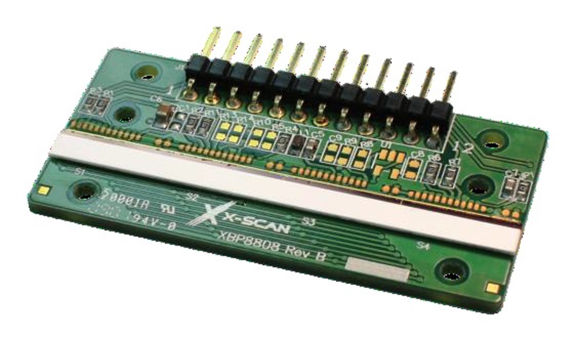
XB Series CMOS X-Ray Line Scan Detector Boards
REQUEST PRICING AND AVAILABILITY
- Get your individual quote.
- Technical compatibility review included.
- Volume discounts available.
No obligation. Direct access to our engineering team.
Downloads
- XB 8850 LDA CMOS X-Ray Line Scan Detector Board X-Scan Imaging Datasheet
- XB90802 TDI CMOS X-Ray Line Scan Detector Board X-Scan Imaging Datasheet
- XB 8801R LDA CMOS X-Ray Line Scan Detector Board X-Scan Imaging Datasheet
- XB 8804R LDA CMOS X-Ray Line Scan Detector Board X-Scan Imaging Datasheet
- XB 8816R LDA CMOS X-Ray Line Scan Detector Board X-Scan Imaging Datasheet
Product information "XB Series CMOS X-Ray Line Scan Detector Boards"
CMOS Photodiode Detector Array; Pixel Size 0.04x0.075 to 1.565x2.4 mm; Resolution 0.05-1.6 mm; 32-6,144 Pixels; Length 51.2-307.2 mm; Scintillator GOS:Tb, CsI:Tl, CdWO4, Other; Data Rate 1 MHz Max.; Dynamic Range >4000
X-Scan Imaging’s XB series are single-chip, buttable silicon CMOS line scan detector boards with on-chip, fully integrated signal processing circuits designed for visible wavelength and x-ray imaging applications.
A scintillator layer is attached to the surface of the photodiode detector array, which converts X-ray photons into visible light. A variety of standard x-ray sensitive scintillator materials are available for applications in industrial inspection, airport security and cargo screening.
Each XB series detector board is configured as a contiguous linear array of photodiodes including a timing generator, digital scanning shift register, an array of charge integrating amplifiers, sample-and-hold circuits and signal amplification chain.
XB series detector boards are designed to permit end-to-end butting on a printed circuit board to form a single longer detector array for extended length scanning applications.
Key Features:
- Element Pitch (Resolution) 0.05 to 1.6 mm
- Pixel Size: 40 x 75 µm to 1.565 x 2.4 mm
- Active Area Length: 51.2 to 307.2 mm
- Number of Elements: 32 to 6,144
- 5 V Power Supply Operation
- Simultaneous Integration by Using an Array of Charge Integrating Amplifiers
- Sequential Readout With a Digital Scanning Shift Register
- Maximum Data Rate: 1 MHz
- Integrated CDS Circuits Allow Low Noise and Wide Dynamic Range up to >4000
- User-specified Scintillator Material: GOS:Tb, CsI:Tl, CdWO4, etc.
- Extended Radiation Hardness Lifetimes (88xxR Series)
Applications: Linear X-Ray Imaging for Industrial and Food Inspection, Homeland Security, Contraband and Cargo Screening, Biological and Industrial CT
Customers also viewed

REQUEST PRICING AND AVAILABILITY
- Get your individual quote.
- Technical compatibility review included.
- Volume discounts available.
No obligation. Direct access to our engineering team.

REQUEST PRICING AND AVAILABILITY
- Get your individual quote.
- Technical compatibility review included.
- Volume discounts available.
No obligation. Direct access to our engineering team.