REQUEST PRICING AND AVAILABILITY
- Get your individual quote.
- Technical compatibility review included.
- Volume discounts available.
No obligation. Direct access to our engineering team.
Product information "VTA Series Photodiode Arrays"
Active Area 0.50-5.20 mm²; Pitch 0.8-2.5 mm; No. of Elements 16, 32, 64; Scintillator Crystal Type Csl, GOS, Custom; Radiometric Sensitivity 0.30 A/W; Max. Junction Capacitance 100-600 pF; Max. Dark Current 50-100 pA
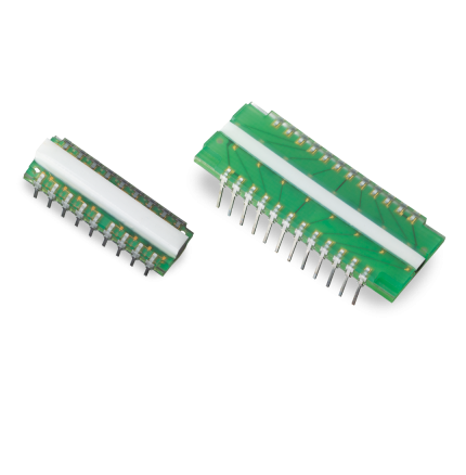
With the VTA Series, AMS Technologies offers a wide variety of Excelitas standard catalog photodiode arrays. With standard pitch values from 0.8 mm to 2.5 mm, you are sure to find the right detector for your X-ray imaging needs.
The VTA Series photodiode arrays are used to generate an X-ray image by scanning an object line by line. The X-rays are converted into light through the attached scintillator crystal. The light intensity is then measured by the photodiodes. The boards are employing chip-on-board technology with optically adapted scintillator crystals. 16, 32 or 64 single-element photodiodes are mounted directly on an FR-4 printed circuit board (PCB).
A molded encapsulant of X-ray radiation hard, transparent coating material covers the photo-sensitive chip area while a glob top encapsulant protects the bond wires from damage and environmental influences. These parts are available with or without a scintillator material mounted over the photodiode active area to convert X-rays into visible photons of light.
All “VTAxxxxH-L”-types can be ordered with various scintillator crystals for low energy detection in dual-energy detection architectures and can be paired in such systems with their “VTAxxxxH-H”-series photodiode array counterparts for high energy detection – which again can be ordered with various scintillator crystals for high energy detection.
The designs listed in the table below can be ordered as a standard part but can also be customized to meet the needs of a wide variety of applications. Get in touch with the AMS Technologies photodiode array experts to discuss a solution that matches your project’s requirements.
Excelitas custom photodiode arrays give customers the option to choose the active photodiode area, total number of elements, overall PCB and photodiode chip dimensions, photodiode chip geometry and orientation, electro-optical specifications, single sided vs. double sided PCB, alternative substrate materials (e.g. ceramic) as well as the electrical interface (e.g. connector). First stage amplification electronics can also be added to the custom board design to convert the current generated by the photodiode into an easy to measure voltage.
Applications: Luggage Scanning; Cargo & Container Scanning; Food Inspection; Non-destructive Testing
Please note that Excelitas products are available from us only in Denmark, Finland, Iceland, Norway, and Sweden.
Excelitas’ thermal infrared sensors like thermopiles or pyroelectric IR detectors (PIR) are used for motion detection, presence monitoring, temperature measurement and gas detection. Excelitas’ broad portfolio of sensors, detectors and emitters also includes phototransistors, photodiodes, PIN photodiodes, avalanche photodiodes (APD), ambient light sensors, single photon detectors and many more.
The products can be found in a vast array of applications across automotive, consumer products, defense and aerospace, industrial, medical, safety and security and sciences sectors.
Please note that Excelitas products are available from us only in Denmark, Finland, Iceland, Norway, and Sweden.


